Many data acquisition systems require high precision and fast data acquisition to allow the system to detect small signals and to have more sensor channels* in the same system. The more sensor channels, the smaller the shape of the system, and the lower the cost and power consumption. Remote optical communications and medical devices (eg CT scanners) benefit from fast and highly accurate data acquisition systems. In optical power systems (eg, laser pumps), it is necessary to constantly monitor their power levels. In this data acquisition system, for input laser power requiring a dynamic range of ≥90 dB, the laser control loop response time requires a sampling rate of 1 MSPS. In CT scanners, the data acquisition system must have a resolution of 16 b to 22 b in order to process X-ray signals over a wide dynamic range of various body tissues. The system requires a large number of photodetectors (more data acquisition channels) and high-precision data acquisition to improve image resolution.
The above two examples illustrate that the system requires relative accuracy rather than absolute precision. Although it is important to detect a power variation of 10 nW with respect to an input optical power of 1 μW, the same 10 nW variation is insignificant as the absolute value of the difference between 1.00001 mW and 1 mW. However, the specification of the accuracy of an analog-to-digital converter (ADC)--integral linearity error (INL) is an absolute error. In order to obtain the best relative accuracy, an innovative solution proposed in this paper is to use a programmable gain amplifier (PGA) in the front end of the precision ADC. The full-scale linearity error of the AD7677 ADC is ±15 ppm (±1 LSB at 16-bit resolution). The settling time at which the PGA of this ADC front end reaches a steady state must be fast enough to match the conversion speed of an ADC with the same resolution. In addition, the PGA must also have as low a noise as possible because it determines the signal-to-noise ratio (SNR) of the data acquisition system. To solve these problems, the amplifier in this design uses the AD8021 operational amplifier, which has the speed, accuracy, and fast settling time to meet the design requirements, and its voltage noise spectral density is only 2 nV/√Hz. Figure 1 shows the correspondence between the PGA gain setting and its ADC accuracy. The system achieves a 19 b accuracy when the input signal amplitude is low.
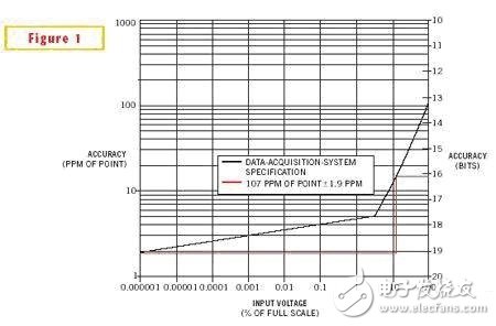
Figure 1 Using a PGA on the front end of a 16-bit ADC improves its accuracy to 19 bits.
The relative accuracy of the ADC is usually the maximum deviation between the actual value and the theoretical value of the analog quantity corresponding to any digital quantity when the full scale range is calibrated, expressed in parts per million (ppm) of the relative fullness range. (Also available as a percentage, or LSB), plus (±) the ppm corresponding to the minimum absolute error caused by the system measurement process. The circuit design shown in Figure 2 achieves a relative accuracy of 107 ppm ± 1.9 ppm. The analog multiplexer IC4 contains multiple channels with smaller bandwidths to take advantage of the ADC's 1MSPS sample rate. Because the PGA exhibits a high input impedance to the multiplexer, multiple multiplexers can be cascaded to increase the number of channels. The multiplexer also has a calibrated input port that makes it easy to calibrate the offset voltage and gain error caused by each gain setting with a single calibration reference. Calibration only needs to be done when power is applied or when operating conditions (eg, temperature) change. The amplification link consists of a multiplexer, comparator, preamplifier, and ADC. The AD7677 has a successive approximation structure that allows individual parts of the amplified link to operate simultaneously. When the ADC samples a channel, its comparators and amplifiers stabilize the subsequent channels. Therefore, the data acquisition system can operate at the maximum sampling rate of the ADC.
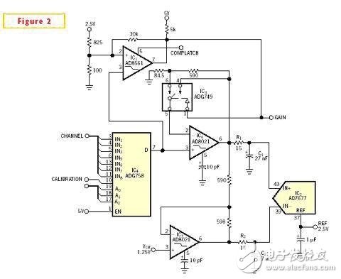
Figure 2 combines a PGA with a 16-bit ADC to provide 19-bit accuracy
After the analog multiplexer has stabilized, the fast comparator IC1 immediately completes the appropriate gain setting. The comparator's threshold voltage causes the signal to be amplified and clamped without being amplified by IC6 and IC7. With a response time of 7 ns, the AD8561 comparator provides a lockout signal that maintains the gain during the amplifier's stabilization period and during ADC capture. A typical PGA configuration requires the user to pre-set the gain of the amplifier before applying the signal to the input. The PGA in Figure 2 features an "automatically set gain range" that selects the most appropriate PGA gain for maximum accuracy without signal saturation or clamping. The comparator includes a hysteresis circuit to reduce the set gain variation as the signal approaches a particular gain range limit. The circuit automatically increases the accuracy of the ADC to 19 bits while maintaining its full-speed sampling rate of 1 MSPS.
IC6 uses a gain setting of 1 or 8 to amplify the output signal of the multiplexer. If a different gain of up to 25 is required, the feedback network resistance can be changed. The analog switch IC3 controls the setting of the gain. The high gain bandwidth product of the AD3801 op amp provides enough bandwidth so its compensation capacitor remains the same for all gains. Amplifier IC7 produces a differential input signal for the ADC. The settling time of the comparator and amplifier and the capture time of the ADC are much less than the 1μs conversion time of the ADC. The RC noise filters R1/C1 and R2/C2 at the two inputs of the ADC take up extra time. These filters limit the noise bandwidth of the PGA. When the gain of IC7 is -1, PGA is the main noise source of the data acquisition system.
Figure 3 shows the linearity error of this circuit design. It is not easy to achieve such a low linearity error at this highest gain setting (the maximum is 0.44 LSB and the minimum is -0.37 LSB). This is equivalent to a typical error of ±0.9 ppm. When the gain is 8, the output noise is 85 μV rms. If needed, you can use software to further reduce noise evenly. Figure 4 shows a complete data acquisition system using the AD7677* evaluation board with a printed circuit board area of ​​15 x 30 mm.
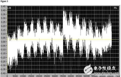
Figure 3 Linear error of the data acquisition system for all possible ADC digital quantities
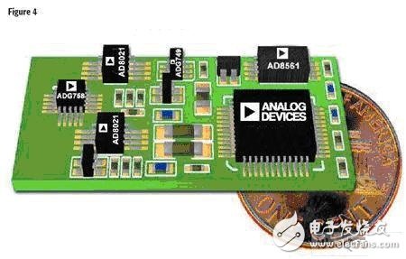
Figure 4 Relative dimensions of a complete data acquisition system with reference to a 1 cent coin
Outdoor Front Service LED Display
Front Service Outdoor Fixed Install LED Display Screen
1. High refresh rate: With NOVA STAR control system, no scanning line when photographed
2. High gray level: 256 RGB each ,display 16.7M colors ,vivid and perfect video effect
3.High resolution: The most apparent features of the new generation of LED display
4.Good color uniformity
5. High Brightness: 6000-8000 cd/m2 ,brightness automatically adjusted
6. High Quality: CE, RoHs, FCC, UL, IP65, ISO9001 passed + 96 Hours serious testing time
7. Long life span: over100,000hours, warranty from 2 years.
* Nova MSD 300 sending card and Nova mrv328 receiving card
* Cabinet size:960x960mm
* Kinglight/Nationstar LED Lamp, Refresh rate:1920-3840hz
* Ultra-Light designing, less than 30kg/pcs
* High brightness up to 6500cd/sq.m, even in the sunlight conditions can see clear, but low power consumption to save the electric power cost.
* High debugging brightness and no damage to gray scale, achieving the debugging technology for nice image.
* Passed the TÃœV,FCC,ROHS,CE cetification.
Outdoor Front Service LED Display,P3.91 Outdoor Led Screen,Led Stage Screen
Guangzhou Chengwen Photoelectric Technology co.,ltd , https://www.cwledpanel.com