Recently, a team of scientists from Boston University, Massachusetts Institute of Technology, University of California, Berkeley, and Boulder School of the University of Colorado developed a new manufacturing solution to integrate photonic devices with electronic devices on bulk silicon substrates. Come together.
background
At present, there are bottlenecks in the transmission of electrical signals from microelectronics chips. Transmission speed and distance are limited by the traditional method of transmitting data through wires, and both energy consumption and heat generation are great. Nowadays, electronic devices are tending to higher performance and lower power consumption, and the bottleneck of traditional methods is increasingly prominent.
In order to overcome this bottleneck, optical data transmission is expected to be one of only a few candidate solutions. The data transmission rate of the optical fiber is nearly 1000 times that of the electric wire, the energy consumption is relatively low, can also send higher frequency data. In optical fiber, you can use a variety of different colors of light, and each color of light has a data channel. In addition, the optical fibers can be packed more closely together than copper wires, and there will be no cross talk between telecommunications channels.
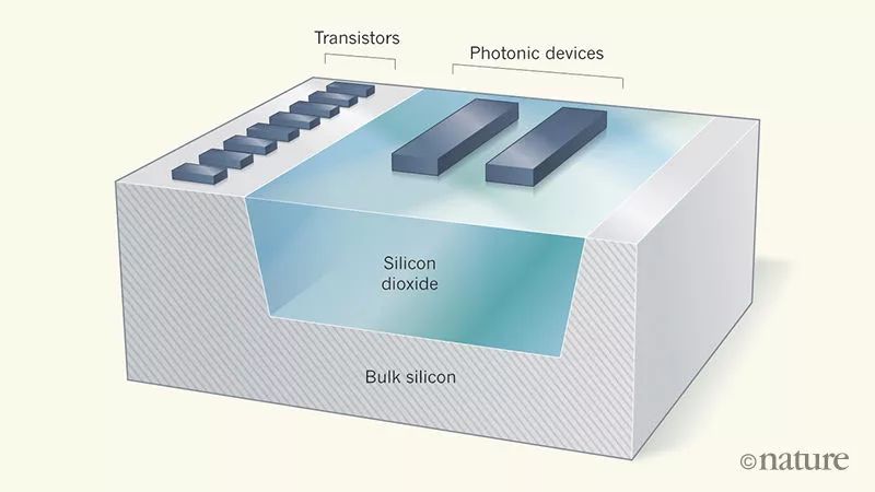
However, the integration of electronic devices and photonic devices on a single silicon chip is constrained by existing semiconductor manufacturing processes. Specifically, the material platforms used for silicon electronic devices and photonic devices cannot be compatible with each other. Most electronic devices use bulk silicon substrates, while photonic devices use silicon-on-insulator (insulator) platforms. .
Innovation
Recently, a team of scientists from Boston University, Massachusetts Institute of Technology, University of California, Berkeley, and Boulder School of the University of Colorado developed a new manufacturing solution to integrate photonic devices with electronic devices on bulk silicon substrates. Come together. On April 19, related papers were published in the journal Nature.

(Source: Amir Atabaki)
The research results began with a project for several years that was sponsored by the US Department of Defense Advanced Research Projects Agency, led by Vladimir Stojanovic, associate professor at the University of California at Berkeley, Rajeev Ram, professor at MIT, and Milos Popovic, assistant professor at Boston University. They also collaborated with the Semiconductor Manufacturing Research Group of the School of Nanoscience and Engineering (CNSE) at the State University of New York in Albany.
technology
In 2015, the first major effort to overcome the bottleneck in chip electrical signal transmission was born. The research team described the results in another paper published in the journal Nature. However, this solution can only be applied to a small number of the most advanced microelectronics chips, and cannot be applied to the most popular chips using bulk silicon substrates.
(Source: CNSE Albany)

(Source: Nature)
value
This new platform brings photonic devices into the most advanced bulk silicon microelectronics chips, bringing faster and more energy-efficient communications, and will pave the way for mass production of optoelectronic subsystem chips, greatly improving computing devices and mobile devices. .
In addition to traditional data communication, its applications include deep learning neural network training in image and data recognition tasks, low-cost infrared lidar sensors used in driverless cars, smart phone face recognition technology, and augmented reality technology.
In addition, the optically enabled chips will bring new types of data security and hardware authentication, more powerful chips, quantum information processing devices, and quantum computing devices for use in fifth-generation (5G) wireless communication networks.
ZGAR AZ Vape Pods 5.0S
ZGAR electronic cigarette uses high-tech R&D, food grade disposable pod device and high-quality raw material. All package designs are Original IP. Our designer team is from Hong Kong. We have very high requirements for product quality, flavors taste and packaging design. The E-liquid is imported, materials are food grade, and assembly plant is medical-grade dust-free workshops.
From production to packaging, the whole system of tracking, efficient and orderly process, achieving daily efficient output. WEIKA pays attention to the details of each process control. The first class dust-free production workshop has passed the GMP food and drug production standard certification, ensuring quality and safety. We choose the products with a traceability system, which can not only effectively track and trace all kinds of data, but also ensure good product quality.
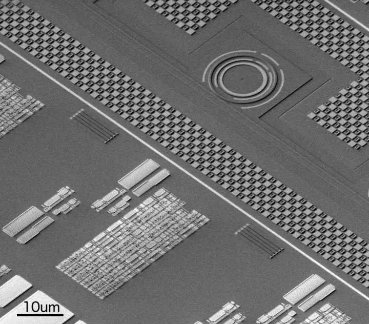
We offer best price, high quality Pods, Pods Touch Screen, Empty Pod System, Pod Vape, Disposable Pod device, E-cigar, Vape Pods to all over the world.
Much Better Vaping Experience!


ZGAR AZ Pods 5.0S Pods,ZGAR AZ Vape Pods 5.0S,ZGAR AZ Vape Pods 5.0S Pod System Vape,ZGAR AZ Vape Pods 5.0S Disposable Pod Vape Systems
Zgar International (M) SDN BHD , https://www.oemvape-pen.com