 Chip manufacturing process The complete chip manufacturing process includes chip design, wafer fabrication, package fabrication, and cost testing, among which the wafer fabrication process is particularly complex. The first is the chip design, according to the needs of the design, generated "pattern."
 1, the raw material wafer wafer wafer composition is silicon, silicon is refined from the quartz sand, the wafer is the silicon element to be purified (99.999%), and then these pure silicon into a silicon crystal rod, become The quartz semiconductor material of the integrated circuit is manufactured and sliced. It is the wafer required for the chip fabrication. The thinner the wafer, the lower the cost of production, but the higher the process requirements.
2. Wafer coating film Wafer coating can resist oxidation and temperature resistance, and its material is a type of photoresist.
3, wafer lithography development, etching The process uses a chemical sensitive to ultraviolet light, that is, in case of UV light becomes softer. The shape of the chip can be obtained by controlling the position of the shade. The silicon wafer is coated with photoresist so that it dissolves in the presence of ultraviolet light. The first shade can then be used so that the portion of the UV light that is directly exposed is dissolved. This dissolved portion can then be washed away with a solvent. The remaining part is the same as the shape of the shade, and this effect is exactly what we want. This gives us the silica layer we need.
4. Impurities are implanted into the wafer to generate corresponding P and N semiconductors.
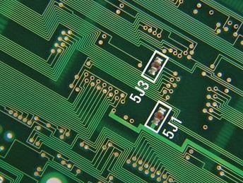
The specific process starts from the exposed area on the silicon wafer and is placed in the chemical ion mixture. This process will change the conductivity of the doped area so that each transistor can turn on, off, or carry data. A simple chip can use only one layer, but a complex chip usually has many layers. At this time, this process is repeated continuously, and different layers can be connected through the open window. This is similar to the production principle of multi-layer PCB. More complex chips may require multiple layers of silicon dioxide. This is achieved by repeating lithography and the above process to form a three-dimensional structure.
5. Wafer Test After a few processes above, a grain is formed on the wafer. The electrical characteristics of each die were measured by needle testing. In general, the number of crystal grains owned by each chip is enormous. Organizing a pin test pattern is a very complicated process, which requires production of a large-volume production model with the same chip size as possible. The greater the number, the lower the relative cost, which is why the cost of mainstream chip devices is low.
6, the package will be manufactured to complete the wafer, bind the pins, according to the requirements to be made into a variety of different forms of packaging, which is the same kind of chip core can have different packaging forms reasons. For example: DIP, QFP, PLCC, QFN and so on. This is mainly determined by the user's application habits, application environment, market form and other external factors.
7. Testing and Packaging After the above process flow, the chip production has been completed. This step is to test the chip, reject defective products, and package.
Printed Circuit Board,Pcba Circuit Board Direct,Pcba Circuit Board,Pcb Gold-Plated Circuit Board
Shenzheng Weifu Circuit Technology Co.Ld , https://www.wfcircuit.com