First, DSP-based USB interface design
1 Introduction
The data processed by the DSP is often transmitted to the PC for storage and reprocessing, so the high-speed communication problem between the DSP and the PC must be solved. This design scheme uses Texas Instruments' C5000 series DSP chip TMS320VC5416 as the microprocessor. It uses the USB2.0 interface chip CY7C68001 provided by Cypress to realize the USB2.0 slave interface design, so that the PC and DSP pass USB2. The 0 interface enables high-speed bidirectional transmission of data.
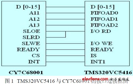
2 TMS320VC5416 and CY7C68001 EZUSBSX2 hardware interface design
The system solution uses a PC as the host computer, which is responsible for detecting the device access and enumerating and identifying on the USB bus, and can control the data transmission by running an application on the PC. The USB chip acts as a USB device end and connects the data exchange between the DSP and the host computer. DSP is used to implement USB protocol. DSP data is used to realize DSP data communication with PC through USB interface, and the descriptor writing of USB chip and the processing of various command states are realized by DSP programming.
The TMS320VC5416 is a 16bit fixed-point high-performance DSP from TI. Due to its low power consumption and high performance, the VC5416's separate instruction and data space allows the chip to have high parallel operation capability, allowing simultaneous access of instructions and data in a single cycle. In addition, the highly optimized instruction set makes the chip highly computationally fast, and the chip itself has a wide range of on-chip memory resources and a variety of on-chip peripherals, so it has been widely used in the engineering community.
Cypress's CY7C68001 EZ-USB SX2 is a high-performance, easy-to-use USB 2.0 interface chip that satisfies the USB 2.0 protocol and works in high-speed (480Mbps) or full-speed (12Mbps) mode, providing a control endpoint for Requests for handling USB devices and four configurable endpoints for transport control and data signals. These four endpoints share a 4KB FIFO space with a standard 8-bit or 16-bit external host interface for seamless connection to multiple standard micro Processors, such as DSP, ASIC, and FPGA, can be set to synchronous or asynchronous interfaces according to requirements, and integrated on-chip phase-locked loop (PLL). The chip is widely used in DSL modems, MP3 players, card readers, and digital cameras. , scanners, printers and other equipment.
The hardware interface design of the system is shown in Figure 1 and Figure 2. The two communicate through the data, address bus, and read and write signal lines. The chip select signal of CY7C68001 is connected to the I/O space chip select signal of TMS320VC5416, CY7C68001. The FIFO is extended on the I/O space of the VC5416.
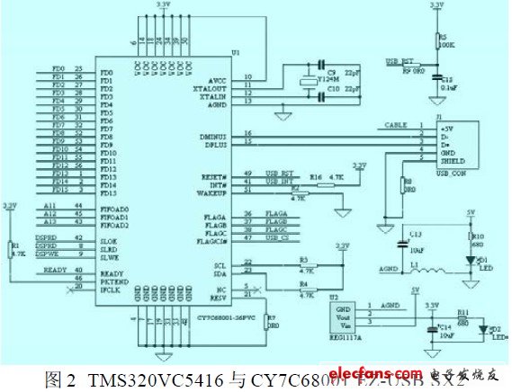
The power supply part uses a 1117 to convert 5V to 3.3V to supply CY7C68001EZ-USB SX2. The magnetic ground is connected between the analog ground and the digital ground. The reset part adopts the RC circuit design, and the typical data is 100KΩ and 0.1μF.
3 interface operation principle
The CY7C68001 has two external interfaces:
(1) Command interface: used to access the CY7C68001 register, Endpoint 0 buffer, and description table.
(2) FIFO data interface: used to access data in four 1K byte FIFOs.
Both external interfaces can be accessed synchronously or asynchronously.
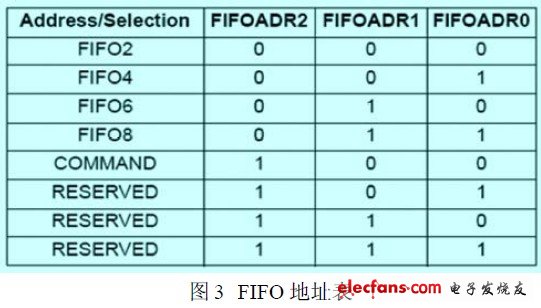
This design is accessed asynchronously. According to the address allocation of Figure 3, the three high-order address lines (A11, A12, A13) of TMS320VC5416 are used to connect FIFOAD0/1/2 of CY7C68001 to select FIFO2, FIFO4, FIFO6, FIFO8 and command interface. The address table is shown in Figure 3. Shown. When the address line FIFOADR[2:0] of CY7C68001 is 100B, the command port (Command) of CY7C68001 is selected. Through the command port of CY7C68001, you can access 37 registers, Endpoint 0 buffer (64 byte FIFO) and description table (500 bytes FIFO). The read and write modes of these registers are secondary addressing mode. First, the subaddress and operation type (read or write) of the register to be addressed are written through the command port, and then the data is read or written to the corresponding register through the command port.
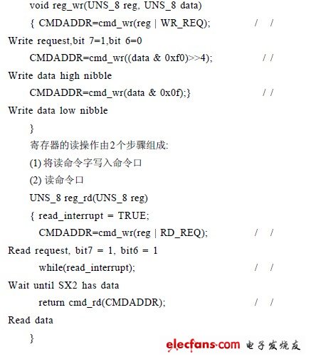
The contents of the write command port are called command words. The command word contains the subaddress of the register to be addressed, or the upper 4 bits or lower 4 bits of the data to be written to the register. The read command port must be followed by the read command word to the command port, and the 8-bit data of the corresponding register is read. Therefore, the write operation of the register consists of 3 steps:
4 USB interface software design
The software design of the USB interface consists of two parts: one is to run the USB 2.0 UTIlity tool in the PC Windows, which is a Windows graphical user interface software that provides the interface program between CY7C68001 and the Windows operating system, making the development of CY7C68001 simple. The second is to run the embedded application code in the DSP, provide hardware drivers, manage CY7C68001 for different ways of data processing, thus implementing the USB2.0 transmission protocol.
4.1 USB interface software design process
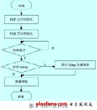
USB interface software design, DSP-side code roughly includes DSP chip initialization (vc5416_init function), USB chip initialization (sx2_init function), USB chip configuration program (sx 2 _ setup function) and USB chip data read and write program (sx2_processdata function), The program flow is shown in Figure 4.
DSP chip initialization (vc5416_init function) is mainly responsible for setting the operating frequency of VC5416, configuring SWCR and SWWSR registers. In addition, this application system uses a GPIO pin as the reset signal of 68001, so it needs to be related.
The USB chip initialization (sx2_init function) is mainly responsible for clearing the Buffer buffer and enabling the external interrupt INT1 of the VC5416. After the initialization is completed, the READY interrupt is issued. At this time, the DSP writes the descriptor to 68001, and performs an enumeration process. After the enumeration is passed, The ENUMOK interrupt is issued. The enumeration mode can be externally imported by the external EEPROM through the I2C bus, and can be imported from the DSP to the 68001 by running the DSP program. The application system uses the second enumeration method.
The USB chip configuration program (sx2_setup function) is a program that is executed after the command channel (0 node) receives the upper computer request that cannot be processed automatically, and 68001 issues a SETUP interrupt to the VC5416. At this time, the VC5416 performs eight read operations continuously to the SETUP register. The process can get an 8-byte request, and the system can respond to the request or STALL the request.
The USB chip data read/write program (sx2_processdata function) means that the PC and the USB slave device communicate with each other in accordance with the USB transfer protocol.
When the address FIFOAD[2:0] of CY7C68001 is 100, the command interface of CY7C68001 is selected. The read and write of the command interface is performed in two steps. That is, when the READY is valid, the subaddress and the operation type (read or write) of the register to be addressed are first written through the command interface, and then read twice when the READY is valid again. Write a command interface to read and write one byte of data.
4.2 Interrupt service program design points
The DSP uses an external interrupt pin (INT1) to connect to the INT pin of CY7C68001. A series of activities on the USB bus will trigger the corresponding interrupt. Once the interrupt is generated, the DSP will read the corresponding value from the Command port of CY7C68001. To determine what kind of interruption is generated.
CY7C68001 EZ-USB SX2 includes six interrupt sources: SETUP (interrupt generated when a Set-up packet is sent from a USB host computer (PC)), EP0BUF (interrupt generated when endpoint 0 buffer is available), FLAGS ( OUT Endpoint FIFO status is changed from empty to non-empty), ENUMOK (interrupt generated after SX2 enumeration is completed), BUSACTIVITY (interrupt generated when SX2 detects bus activity), and READY (SX2 is powered up and reset is completed) After the interrupt is generated, each interrupt source can be enabled or disabled by setting or clearing the corresponding bit in the INTENABLE register.
The CY7C68001 chip uses an interrupt buffering mechanism. There will only be one interrupt source at a time. Other interrupt sources will only issue new interrupt requests after the previous interrupt has been read.
Therefore, when an interrupt is generated, the INT pin is in a low state, and the interrupt status bit is placed in the command interface. After entering the interrupt program, the interrupt source should be judged first. First, it is judged whether it is the interrupt generated by the read register. If yes, the data is ready to be set to flag 1 and then returned. Otherwise, the external PC reads the interrupt status bit from the command interface by strobing the SLRD/SLOE signal to determine which interrupt is generated, and then performs the corresponding operation according to the interrupt source. The DSP automatically clears the interrupt flag bit after reading the interrupt status bit.
5 Conclusion
Through the construction of the hardware platform and the realization of the software program, it is verified that the interface circuit can meet the data transmission requirements of high-speed signal processing, and has the advantages of high speed and high reliability.
1000W Portable Power Station,1000W Power Station,Solar Power Generator,Camping Power Bank
Guangzhou Fengjiu New Energy Technology Co.,Ltd , https://www.flashfishbattery.com