Serial interfaces are commonly used for chip-to-chip and board-to-board data transfers. As system bandwidth continues to increase to the multi-gigabit range, parallel interfaces have been replaced by high-speed serial links, or SERDES (serializer/deserializer). Initially, SERDES was a standalone ASSP or ASIC device. In the past few years, a family of FPGA devices with built-in SERDES has been seen, but it is more common in high-end FPGA chips and is expensive.
This solution is based on CME's latest low-power series FPGA HR03 platform, which realizes 8/10b SerDes interface, including SERDES transceiver unit, realizes CDRDES CDR (Clock Data Recovery) by completely digital method. 100~200Mhz inter-board SERDES single-channel communication, the SERDES interface solution features low cost, high flexibility, and short development cycle.
1 hardware interface:
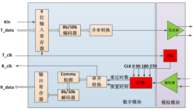
The interface of the hardware is as shown in the figure above, mainly including the transmitting and receiving modules.
The transmitting module includes an 8b/10b encoder, a parallel-serial converter, a phase-locked loop (PLL) frequency synthesizer and a transmitter, and a receiving module including an 8b/10b decoder, a Comma detector, a serial-to-parallel converter, and a clock data recovery device ( CDR) and receiver.
The 8b/10b encoder is used to map the byte signals sent from the upper layer protocol chip to the DC balanced 10-bit 8b/10b code, and the serial conversion is used to serialize the 10-bit coded result and the high speed required for serial conversion. The low-jitter clock is provided by a phase-locked loop, and the transmitter is used to convert a CMOS-level high-speed serial code stream into a differential signal with strong anti-noise capability, and transmit it to the receiver via a backplane connection or a fiber channel.
At the receiving end, the receiver restores the received low-swing differential signal to a CMOS-level serial signal. The CDR extracts the clock information from the serial signal to complete the optimal sampling of the serial data. The serial-to-parallel conversion utilizes the CDR. The recovered clock converts the serial signal into 10-bit parallel data. The Comma detector detects special Comma characters, adjusts the word boundary, and corrects the parallel data of the word boundary. It is decoded by 8b/10b, restored to a byte signal, and transmitted to the upper layer. The protocol chip completes the entire information transmission process.
In the actual design, the CDR part is completed by pure logic circuit, which is the core part of the design. The implementation of digital CDR in HR03 will be introduced below.
2 digital CDR:
The role of the CDR module is to recover the embedded clock from the data, and then the receiver aligns the data bits according to the recovered clock and aligns the words by comma. Finally, the data is decoded 8b/10b for use by the system.
This scheme adopts the same-frequency multi-phase clock sampling method. The specific implementation process uses the PLL to generate four clocks with the same clock frequency and phase difference of 90 degrees, which are clk0, clk90, clk180 and clk270 respectively. These four clock outputs are completely synchronized and utilized. The four clocks sample the data to obtain the effect of 4 times oversampling. The specific implementation process is as follows:
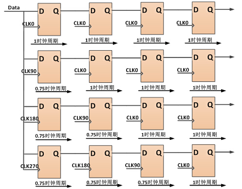
When the data clock is recovered, the incoming data is input to four flip-flops, respectively, and sampling is performed with four different phases. Care must be taken to ensure that the delay from the input pin to the four flip-flops is substantially the same.
The triggering of the first column of flip-flops is triggered by the rising edges of the clocks CLK0, CLK90, CLK180, and CLK270, respectively, and four data sampling points can be obtained by triggering in this manner. This divides the original clock cycle into four separate 90-degree regions. If the system clock is 200 MHz, the circuit shown above is equivalent to producing a sampling rate of 800 MHz.
Only through the first-order flip-flop, the output sample data has a metastable problem, so the sample points need to be further processed. Here, the four sampling points can be further triggered to remove the metastable problem, thereby moving the sampling point to the next identical clock domain. Usually, the removal of the metastable state is processed by two or three levels, which causes digital invalid data before the effective data output. In the first stage of data sampling, the circuit detects the data transmission on the data line. When the data transmission is detected, the validity of the transmitted data is confirmed. After confirming that the data is valid, the output is high to indicate that the sample point has data transmission.
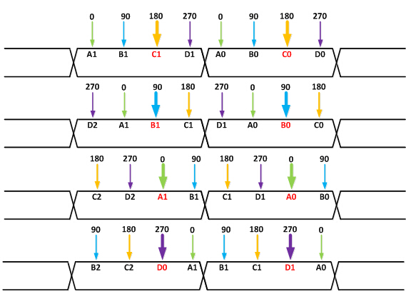
Because there are ultimately four outputs, a multiplexer is needed to select the data. The correspondence between the transmitted data and the sampling clock is as shown in the figure above. The corresponding relationship is divided into four cases. In each case, an optimal sampling clock is used. The system determines the clock by determining the edge information of the data edge. The best sampling clock, and the multiplexer is used to select data bits from the selected clock domain. For example, the detecting circuit determines that the data sampled from the clock domain A is valid, and then the data sampled in the clock domain A is output through the output terminal.
3 Conclusion:
Through the CDR circuit of the pure digital circuit, without the support of the hard core, the interface design of the SERDES on the FPGA is completed, and the experimental transmission test can complete the data transmission of 100~200 Mbps on the HR03 FPGA.
Author: Beijing Jager micro system engineers easily Jingjing
Today let`s talk about touch screen laptop. Sometimes people take Yoga Laptop or 2 In 1 Laptop or 360 Laptop as foldable touch screen laptop. Cause the later ones usually with touch screen function. The difference is that touch screen laptop specials can`t be flipped up to 360 degree, usually 180 degree. Do you think which kind of person love 2 in 1 touch screen laptop more? Business people is the right answer, cause they care more performance, touch screen function, 180 rotating, which are the very important points for businessman, especially teaching in person, do presentation, etc.
Do you think what other business laptop businessman love also except touch screen laptop under 20000? 14 inch 11th Laptop and 15.6inch 11th or 10th Laptop should be the top levels.
As a professional manufacturer, also customizing Android Tablet, Mini PC , and all in one except laptop. So believe you can always get the most competitive one at this store, balancing the quality and cost at top.
Any other special demand, you can just contact us freely. Will try our best to back you up.
Touch Screen Laptop,Touch Screen Laptop Specials,Touch Screen Laptop Under 20000,Foldable Touch Screen Laptop,2 In 1 Touch Screen Laptop
Henan Shuyi Electronics Co., Ltd. , https://www.shuyilaptop.com