Introduction
IO-Link is a communication standard for point-to-point three-wire interfaces for smart sensors and actuators in industrial applications. IO-Link extends the traditional interface capabilities of these devices from a simple NC/NO switch interface (standard IO or SIO mode) to a two-way intelligent interface that can pass three different speeds (COM1 - 4.8kb/s, COM2 - 38.4) Kb/s or COM3 — 230.4kb/s) One of the code conversions to send additional information. In addition to the data pins (C/Q), the IO-LinkType A interface has a 24VDC power supply pin (L+) and a common return pin (L–).
Â
When an IO-Link master powers up, it asks each connected device to determine the correct operating mode for each device: SIO, COM1, COM2, or COM3. This allows legacy legacy devices and devices that support the IO-Link standard to work seamlessly in the same system.
Â
The LTC2874 has a rated CQ output current of 110mA. Higher currents of up to 440mA can be achieved by connecting multiple channels in parallel. While this exceeds the IO-Link standard specification limits, some non-standard SIO applications may require a larger current supply and/or the need to maintain the functionality of four independent channels. This article shows how to change the use of the LTC2874 hot-swap channel to provide a large current for the SIO load (called SIO+ mode) while maintaining the IO-Link features and functionality of the LTC2874.
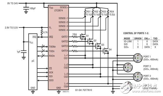
Figure 1 : LTC2874  Four channels  IO-Link master configuration having three high current Â
SIO port (SIO +) and L + 1 with hot-plugging current standard port SIO
Circuit description
As shown  As shown in ports 1–3 of 1, by connecting the hot-swap controller output of the channel to its corresponding CQ pin,  Any large supply current is provided in SIO+ mode. For high current ports, L+'s hot-swap capability is not available; however, for those applications that expect this feature, an external hot-swap controller can be added. As shown in Figure 1  4, not used for SIO output  The LTC2874 hot-swap controller can be used for normal L+ or other purposes.
In normal  In IO-Link or SIO operation, L+  The MOSFET is turned off and the CQ output is passed  TXEN, TXD and  RXD works fine. All IO-Link functions are maintained, including full speed communication and wake-up pulses at COM3 speed.
Â
During SIO+ operation, the L+ MOSFET is controlled through the SPI register interface and CQ is disabled (TXEN is low or under SPI register control). The upper half of Register 0xE is responsible for controlling the L+ MOSFET. In SIO+ mode, the switching frequency is limited to approximately COM1 speed.
Â
although  LTC2874 in CQ and  The L+ output will not be damaged while it is in operation, but it is not recommended to perform this mode of operation because the rising and falling trajectories of the output waveform are non-monotonic. These traces occur due to timing differences between the channels and the interaction of various current limits and source resistances.
Â
The maximum output current of SIO+ mode is determined by the choice of MOSFET and sense resistor RS. The current limit is set by 50mV/RS. The typical current limit for the circuit in Figure 1 is 500mA. Taking into account tolerances and variations, a 400mA port rated output current is generated. The appropriate MOSFET must be chosen to handle voltage, current, and safe operating area (SOA) requirements. See the LTC2874 product brochure for more details.
Â
MOSFET output capacitance  The 1nF maximum allowed by the IO-Link standard contributes approximately  60pF.
Â
Since the circuit has two drivers in parallel, the idle drive acts as a capacitive load on the working drive. When the working drive changes state, it will generate a charging current in the idle drive. Due to the large capacitance of the MOSFET  The faster edge rate of the CQ drive, so this effect is more pronounced during IO-Link operation. To prevent the charging current pulse from ringing when the working driver is turned off, minimize the MOSFET source and  Parasitic inductance between C/Q driver outputs.
Â
Figure  2 and Figure 3 show a single support  SIO+ mode port drives a resistive load, working simultaneously on SIO+ or normal  Operating waveform in IO-Link mode. The supply voltage is 24V and the resistive loads are 56Ω and 200Ω, respectively.
Â
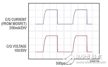
Figure 2: SIO+ operation
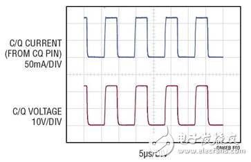
 Figure 3 : IO-Link operation (C/Q) for a port that supports SIO+ mode  At COM3  Speed )
in conclusion LTC2874 works on  The arbitrarily large current of the SIO+ mode can be obtained by changing the hot-swap channel to a higher current SIO driver.
 PTC Thermistor for Overcurrent Protection for Telecom
PTC Thermistor ,Thermistor,Thermistor for Overcurrent Protection ,PTC Thermistor YZPST
YANGZHOU POSITIONING TECH CO., LTD. , https://www.pst-thyristor.com