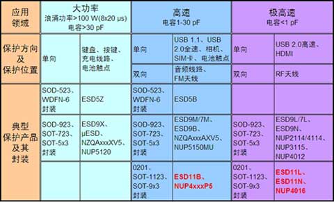
With more features in portable devices such as mobile phones, potential input/output (I/O) channels for electrostatic discharge (ESD) voltage entry are numerous, including keyboards, buttons, SIM cards, battery charging, USB interfaces, ESD protection is required for many locations such as FM antennas, LCD displays, headphone jacks, and FM antennas. Depending on the capacitance and data rate, ESD protection applications for portable devices can be divided into three types: high power, high speed and very high speed. The capacitances are greater than 30 pF, between 1 and 30 pF and less than 1 pF. See Table 1. As can be seen from the table, the higher the speed, the lower the capacitance required for the application, because higher speed applications need to maintain signal integrity and reduce insertion loss.
This article refers to the address: http://
Table 1: ESD protection application classification and typical protection products for portable devices (where red font is the leading product).
The most effective ESD protection method for portable devices
From the perspective of protection methods, one possible option is the on-chip ESD protection, but the shrinking CMOS chips are increasingly insufficient to withstand the area required for internal 2 kV ESD protection, so truly effective ESD protection cannot be completely Integrated into CMOS chips. In addition, although some functions can be played by working in physical circuit design and software design, there are always some important circuits that are sensitive and difficult to isolate from the outside. Therefore, the most effective ESD protection method is still in the connector of portable devices or A protective component is placed at the port to clamp the very high ESD voltage to a lower voltage to ensure that the voltage does not exceed the breakdown voltage of the oxide in the integrated circuit (IC), protecting the sensitive IC.
Under normal operating conditions, the external ESD protection component should remain inactive without any effect on the functionality of the electronic system, which can be achieved by maintaining low current and low capacitance values. In the case of ESD stress shock or high current surge, the first requirement of the ESD protection component is that it must work properly, with low enough resistance to limit the voltage of the protected point; secondly, it must be able to move quickly. In order to make the rise time less than the nanosecond ESD impact rise time.
Comparison of external protection components and their performance test
Common external protection components are varistors, polymers, and silicon transient voltage suppressors (TVS). The materials used are metal oxides, polymers with conductive particles, and silicon. The varistor exhibits high resistance at low voltages and decreases at higher voltages. Polymers with conductive particles have a relatively high electrical resistance at normal voltages, but when subjected to ESD stress, small gaps between conductive particles can become an array of glitch pitches, resulting in a low resistance path. TVS is a silicon chip component designed with standard and Zener diode characteristics. TVS components are optimized for the ability to carry large currents with low dynamic resistance. Since TVS components are typically produced in an IC fashion, we can see a wide variety of single-chip products that are unidirectional, bidirectional, and array-arranged.
Among these kinds of external protection components, TVS components have excellent high-current conductivity and maintain excellent performance under repeated stress conditions. There is no performance degradation after the use of other protective components such as varistor or polymer. The problem, and the new ESD components have extremely low capacitance, making them ideal for ESD protection of high-speed data lines. The higher the speed of the application, the more ESD protection components are required to have lower capacitance and lower clamping voltage.
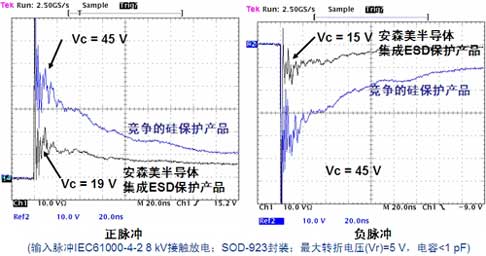
Figure 1: ON Semiconductor's integrated silicon ESD protection components have better clamping voltage performance than competing devices.
The electronic system must be able to survive the IEC 61000-4-2 standard test conditions. In order to make a more direct comparison of the above several external ESD protection components, the varistor, polymer, ON Semiconductor silicon protection component and the closest silicon competing device are first applied IEC 61000-4-2 ±8 The kV ESD contacts the discharge pulse and compares its ESD clamp voltage waveform with an oscilloscope. It can be found that ON Semiconductor's silicon ESD protection component has a much lower clamping voltage, which is not only superior to passives such as varistor and polymer. The component is better than the silicon competing device with the closest performance, see Figure 1.
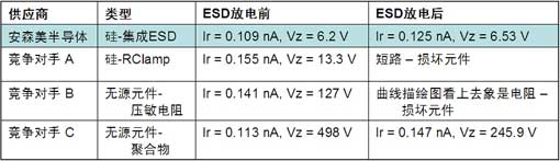
In addition, portable devices may experience multiple ESD voltage stresses, which are prominent in northern China. Because the performance of external protection components in a variety of ESD stress conditions is important, directly determines the reliability of portable products. Therefore, it is also possible to test protective components such as varistor, polymer and silicon ESD diode under Tesec DC test conditions, each of which applies a total of 2,000 15 kV contact discharge ESD pulses (forward and negative for each 1,000). Times), the interval between each pulse is 0.1 second. The test results shown in Table 2 show that ON Semiconductor's silicon-integrated ESD protection components maintain excellent performance under multiple stress conditions, while competing devices are either damaged or have a severe performance degradation.
Table 2: Performance comparison of different ESD external protection components after multiple stresses under Tesec DC test conditions.
ON Semiconductor's high-performance ESD external protection components overview
As shown in Table 1, ON Semiconductor offers a range of high-performance silicon ESD protection components for high-power, high-speed and ultra-high-speed applications in portable devices to meet different application needs. Among them, ON Semiconductor's ESD11L, ESD11N, NUP4016 (for very high speed applications), ESD11B, NUP4xxxP5 (for high speed applications) are the industry's leading products.
For example, the NUP4016 features an ultra-low capacitance of 0.5 pF per I/O line, making it ideal for protecting high-speed interfaces such as Universal Serial Bus (USB) 2.0 high-speed (480 Mbps) and High-Definition Multimedia Interface (HDMI) (1.65 Gbps). The ESD11L5.0D integrates ON Semiconductor's ultra-low capacitance technology into a 3-pin package to protect two high-speed data lines with a 0.5 pF capacitor, providing designers with a single device solution for protecting D+ and D- lines of USB 2.0 ports. The ESD11L5.0D is also capable of connecting a cathode to a cathode and protecting a single bidirectional line with a 0.25 pF capacitor, making it ideal for protecting high frequency radio frequency (RF) antenna lines.
Both the NUP4016 and ESD11L5.0D can clamp a 15 kV (kV) input ESD waveform to less than 8 volts (V) in nanoseconds, providing the highest level of protection for today's ESD-sensitive integrated circuits (ICs). These silicon devices do not suffer from the wear and tear of passive technology, and after many surge events such as ESD, reliability and performance are not affected.
It is worth mentioning that these high-performance silicon protections from ON Semiconductor not only provide extremely low capacitance and extremely low clamping voltage, but also are extremely small, making them ideal for portable products that require excellent protection in ultra-thin packages. Protection device. For example, the NUP4016 protects four high-speed data lines in a tiny 1.0 mm x 1.0 mm x 0.4 mm SOT-953 package, making it the thinnest ESD protection device for high-speed communication interfaces on the market today.
The ESD11L5.0D is available in an ultra-small 1.0 mm x 0.6 mm x 0.37 mm SOT-1123 package, which is 50% smaller and 20% thinner than comparable solutions on the market in SOT-723 packages. The thinnest high-speed communication, USB 2.0 data and power line and protection ESD devices.
ON Semiconductor also plans to offer ESD devices in 0201 CSP packages as small as 0.6 mm x 0.3 mm x 0.3 mm, protecting a single line with a planar area of ​​only 0.18 mm2 per line.
USB 2.0 high-speed application protection example using ON Semiconductor semiconductor protection components
The USB 2.0 interface is very popular in portable devices and has a very high frequency of use in daily use, so it is necessary to provide reliable ESD protection for high-speed USB interfaces. Figure 2 shows a simplified block diagram of a USB 2.0 high-speed application with a speed of 480 Mbps on both the identification (ID) line and the absence of an ID line.
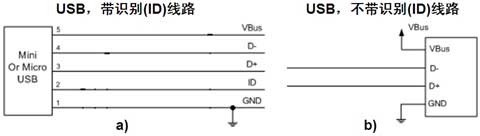
Figure 2: Schematic diagram of USB2.0 high-speed (480Mbps) application structure.
Taking Figure 2 a) with ID line as an example, the application needs to protect 3 high-speed data lines (D+, D- and ID) and 1 high-power line (Vbus) with a device with a capacitance less than 1 pF and a small package. For such protection needs, a discrete protection scheme can be used, such as using three ESD9Ls plus one ESD9X, or an integrated protection scheme such as one NUP3115UP or NUP4114UP (one line is not connected).
In the application of Figure 2 b), it is necessary to protect two high-speed data lines and one high-power line (Vbus) with a device with a capacitance of less than 1 pF and a small package. For such protection needs, you can also use discrete protection schemes, such as using 2 ESD9L plus 1 ESD9X, 1 ESD7L plus 1 ESD9X or 1 ESD11L plus 1 ESD9X, or you can use integrated protection scheme, such as 1 NUP2114UP or 1 NUP4114UP (protects 2 USB ports).
to sum up:
Many locations in portable products such as mobile phones and digital cameras may be affected by ESD pulses and damage integrated circuits in which feature sizes are becoming smaller and more sensitive, thereby affecting system reliability. The most effective ESD protection method is to place external protection components at the connector or port of the portable device. Tests have shown that silicon TVS diodes have better clamping performance than passive components such as polymers and varistors, and ON Semiconductor's silicon protection components are superior to the closest competing devices. As the world's leading provider of high performance, energy efficient silicon solutions, ON Semiconductor offers a broad portfolio of high performance silicon protection components for high power, high speed and very high speed applications in portable devices, many of which are in the industry today. Leading product. These leading products offer extremely low capacitance and very low clamping voltage in a very small package, making them ideal for protecting high-speed applications such as USB 2.0 high speed and HDMI. At the same time, customers benefit from ON Semiconductor's extensive range of silicon protection components, enabling them to flexibly select and match ON Semiconductor's silicon protection components for their USB 2.0 high-speed applications to meet their diverse application needs.
Diode module is called silicon stack, it is made from several diodes in series, the number of the diode is by its highest pressure (maximum) negative peak pressure, main purpose is for high voltage rectifier. China Diode Module,High Voltage Diodes supplier & manufacturer, offer low price, high quality Caterpillar Diode Module,High Frequency Diode Module, etc.
Diode Module,High Voltage Diodes,Caterpillar Diode Module,High Frequency Diode Module
YANGZHOU POSITIONING TECH CO., LTD. , https://www.pst-thyristor.com