With the advancement of digital technology, high-speed, ultra-large-scale integrated circuits are widely used, and 3G mobile terminal baseband signal processing systems are moving toward flexibility, high integration, modularization, and generalization. The baseband signal processor is a combination of digital technology and communication technology. It can flexibly process digital baseband signals and modulate wireless signals to achieve wireless communication with the front-end base stations of the communication network system. This paper designs a 3G mobile terminal baseband signal processor based on advanced microprocessor (ARM), digital signal processing (DSP) and field programmable gate array (FPGA) architecture. The advantage of this architecture is that when providing an advanced processor that better meets the customer's needs, the entire system is easy to integrate, and the functionality can be easily added through software methods without having to customize a new chip for read-only memory (ROM) encoding. At the same time, the system uses software to implement joint detection and signal decoding functions, and it is easy to implement any upgrade of the system through software update without hardware modification.
1 Design ideasWith the development of real-time digital signal processing technology, ARM, DSP and FPGA architecture have become the main way to implement 3G mobile terminals. The design of this paper uses ARM to model and calculate the target and environment, generate network protocol simulation database, apply DSP for data scheduling, operation and processing, and finally form the required control words such as amplitude modulation, phase modulation and frequency modulation, and control and send and receive through FPGA. The chip generates a radio frequency analog signal. By utilizing the versatility between digital chips, the communication between ARM and DSP can not only process the received and transmitted data in real time, but also adapt to the specific requirements of different mobile networks, and at the same time facilitate the loading of new programs. FPGA digital frequency synthesis technology provides a choice for the implementation of RF signal simulation for 3G mobile terminals with its excellent performance in frequency agility speed, phase continuity, relative bandwidth, high resolution and integration.
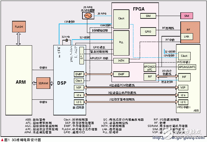
2 hardware implementationThe main part of the system is ARM main control module, DSP real-time data processing module and FPGA signal generation module. The ARM main control module realizes communication between the physical layer and the protocol stack, receives high-level instructions, and performs corresponding tasks. For example, the protocol stack needs to send data to the core network in one or several uplink time slots in some subframes, and receive data of the core network in one or several downlink time slots in some subframes. The instructions and data are stored in Synchronous Dynamic Random Access Memory (SDRAM) and then notified to the DSP for execution. After obtaining the data and commands, the DSP real-time data processing module first processes the transmission data, performs channel coding modulation, CRC attachment, interleaving, spread spectrum modulation, etc., and then processes the received data, such as channel estimation, de-interference, CRC check, channel. Decoding, despreading, Victabit decoding, etc. The FPGA is a signal generation module that manages the 26 M clock, performs the frequency division task, and controls the analog baseband (ABB) automatic transmission power control (APC), automatic receive gain control (AGC), automatic frequency control (AFC), etc. Real-time control of radio frequency (RF) work. When some algorithms in the DSP are very stable, FPGAs can be used to implement these algorithms, reducing the processing load of the DSP. Its hardware circuit is shown in Figure 1.
2.1 Interface
The data exchange between ARM and DSP is realized by two-port random access memory (RAM), that is, the SDRAM in FIG. 1 plays the role of buffering and swapping of uplink and downlink control commands, parameters and data. Here, the number of bits of the dual-port RAM data line is 16 bits, and the SDRAM storage size is 128 M. Hardware interrupt signal line 8 (INT8) and hardware interrupt signal line 9 (INT9) are generated once every 5 ms, which is equal to the sub-frame interrupt of TD-SCDMA air interface signal. It can also be used as ARM and DSP control commands and responses to implement ARM. Communication with the DSP.
The main interface of the FPGA is the data_out[15:0] interface, the digital-to-analog converter (A/D) interface and the RF interface.
The data_out[15:0] interface is used to output the result of the FPGA operation, and is connected with the data bus of the DSP. A three-state gate is set inside the FPGA, and the open signal is the chip select signal CE of the FPGA. When the CE is not strobed, the tri-state gate output is in a high-impedance state and does not affect the DSP's data bus. During each sample interval, the FPGA computes the real and imaginary parts of the correlation value, latches them into four 16-bit latches, and sets the data_ready signal connected to the DSP high. Indicates that the data is ready. After the DSP detects that data_ready is high, it will perform a read operation. The upper bits of the address bus generate a chip select signal to strobe the FPGA, and one of the four latches is selected by the lower two bits A0 and A1 of the address bus. The 32-bit high 16 bits and the low 16 bits of the real and imaginary parts are sequentially read. The FPGA internally counts the read operation of the DSP. After confirming that the data is read out four times, the data_ready is set low until the next operation is completed. The setting of the frequency, phase and amplitude control words of the FPGA and the generation of the control signals are completed by the TMS320C5510. The FPGA can be regarded as an asynchronous storage device connected to the external memory interface (EMIF) of the TMS320C5510. The EMIF uses a 32-bit bus.
The A/D end of the interface with the digital-to-analog converter (A/D) is connected to ABB, and the other end is connected to the FPGA to transmit data to be transmitted and data received by the mobile network. In the interface part with A/D, there are 3 inputs RIF, PS and CLK. RIF is used to serially input the sample value of A/D conversion; PS is the frame synchronization signal, which is used to drive the overall control module inside the FPGA after input to FPGA; CLOCk is the shift clock, which controls A/D and Shift of data serial transmission between FPGAs.
The interface with the RF is mainly used to control the operation of transmitting and receiving RF chips.
2.2 main control module
The main control module is responsible for controlling and coordinating various tasks. ARM adopts the Open Multimedia Application Platform (OMAP) microprocessor produced by TI, and the main frequency of the integrated phase-locked loop multiplier system can reach 66 MHz, and the maximum external storage space can reach 256 MB, rich in on-chip resources, strong peripheral control ability and cost-effective. It controls the DSP module to receive commands and parameters sent by the network to realize wireless free protocol communication.
2.3 Real-time data processing module
The real-time data processing module [1] implements the commands, transmission parameters and data transmitted by the shared memory and the ARM, according to the set working state of the mobile terminal, such as Cell Search, random access procedure (RA), dedicated control channel (DCCH), Real-time dynamic calculation of the FPGA control word with the target and environment. At the same time, the data and information received from the network are also transmitted to the ARM through the shared memory, and the control board is provided with the control attenuation signal to achieve sleep by the latch to save power. The DSP uses the TMS320C5510 from TI's C5000 series. The system clock reaches 600 MHz and the data processing rate can reach 4 800 MIPS. Provides a 32/16 bit host port with two independent external memory interfaces, where EMIF supports 64 bit bus width.
2.4 FPGA module design
The design of this article uses the StraTIx series of chips, embedded in three kinds of RAM blocks of up to 10 Mbit: small RAM of 512 bit capacity, standard RAM of 4 KB capacity, and large-capacity RAM of 512 KB. The FPGA module has a True_LVDS circuit that supports low voltage differential signaling (LVDS), low voltage positive emitter coupled logic (LVPECL), quasi-current mode logic (PCML), and HyperTransport (HyperTranport) differential I/O electrical standards with high speed Communication Interface. This design provides a complete clock management solution with a hierarchical structure and up to 12 phase-locked loops (PLLs). The development software used in the StraTIx series is the new generation development software QUARTus II from ALTEra.
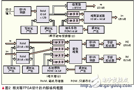
The biggest feature of this series of chips is the programmable DSP module with embedded hardware multiplier and multiply-add structure, which is suitable for high-speed signal processing. This DSP block is a high-performance embedded arithmetic unit that can be configured as a hardware multiplier, adder-subtractor, accumulator, and pipeline registers. With up to 28 DSP blocks and 224 embedded multipliers, the Stratix series provides a flexible, efficient and valuable solution for large data throughput applications. These DSP blocks can implement a variety of typical DSP functions, such as correlator, impulse-limited response (FIR) filtering, fast Fourier transform (FFT) function, and encryption/decryption functions. The correlator algorithm design is implemented by various other algorithms. The foundation and basic components.
The RF signal received by the mobile terminal system is preprocessed by the front end, sent to the A/D sample, and then serially outputs the sample value to the FPGA [2]. Each sample value is represented by a 10 bit two's complement code, which is first converted to a parallel signal with a width of 10 bits by a serial/parallel converter. First, the sample value is to be performed by the Hilbert transform. There are various implementation methods for the Hilbert transform. Here, a 129-order filter is used to implement the filter. The tap coefficient of the filter is generated by the MATLAB function Remez. The other signal is handed over; then the two signals are used as the real part and the imaginary part respectively, and the local sequence is correlated, and the real part and the imaginary part of the correlation value are sent to the DSP for subsequent processing. In this way, the DSP can determine whether to capture the signal by first modulating the correlation value and then judging and further processing the information such as the interval, amplitude and number of peak values ​​of the modulus value. Correlator Algorithm The internal block diagram of the FPGA design is shown in Figure 2.
2.5 PFGA and RF interface, bus and timing control design
The interface, bus and timing control design of FPGA and RF is shown in Figure 3.
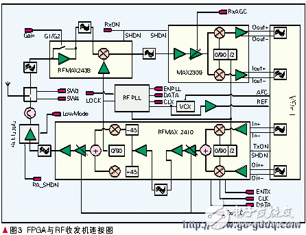
To increase channel capacity and improve bandwidth efficiency, TD-SCDMA combines time division duplexing (TDD) with CDMA by utilizing uplink (reverse link) synchronization, software radio and smart antenna technologies. TD-SCDMA requires that the RF portion of the handset have fast switching times, high dynamic range, and high linearity in the transmitter and receiver sections. The MAX2410 is a complete quadrature transmitter consisting of a quadrature modulator, variable gain IF, and RF amplifier. The MAX2309 is an IF receiver designed for CDMA-based single-frequency single-mode cellular telephone systems with an input frequency range optimized from 70 MHz to 300 MHz, -33 dBm at 35 dBm gain, and +35 dBm gain 1.7 dBm. The FPGA control RF mainly passes through four RF control registers: A word register, B word register, C word register and D word register.
3 software implementationThe mobile terminal software includes application layer software, communication protocol software and physical layer software.
Application layer software LAY 4-7: includes human machine interface (MMI) and system application layer protocol (S/W) part, MMI is mobile terminal user interface, S/W is similar to mobile terminal operating system.
Communication protocol software LAY 2-3: This part of the software is large, mainly for communication protocols, mainly to ensure that the wireless communication system can smoothly communicate in various conditions.
Physical layer software LAY 1: Responsible for coordinating DSP, other hardware and software. The design of the physical layer software will enable energy-efficient features, multiple resources, multi-slot processing, data packets, and monitoring of other network systems. Monitoring of neighboring cells is also required when designing the physical layer software, especially when adjacent cells are not synchronized with each other.
The corresponding functions of each module of the mobile terminal software and hardware are as follows:
Application layer software LAY 4-7 and communication protocol software LAY 2-3 software implementation is mainly implemented in ARM, if LAY 4-7 requires some particularly demanding applications, you can add corresponding hardware modules without affecting The original architecture, such as increasing the processing and playback of high-demand multimedia; physical layer software LAY 1 is mainly implemented in DSP and FPGA.
In software programming, ARM and DSP can be implemented in C language. The debugging tool used is CCS software. When some algorithms in DSP are very mature, when the real-time requirements of mobile communication are relatively high, assembly language should be used. Implementation, in the FPGA can be achieved using the VHDL language. In programming, first try to define the tasks of each functional module, and then define the interface parameters of each functional module, etc., when you can not use global variables, try not to use.
Another major challenge is to implement joint detection algorithms in TD-SCDMA terminals, especially with regard to time optimization of algorithms. There must be a reasonably coordinated division of tasks between the DSP and the FPGA to maximize the functionality of the two processors. In actual software programming, the algorithm program has a large amount of calculation and the encoding delay is too long, so
The algorithm needs to be optimized under the premise of ensuring quality. After satisfying the accuracy requirements, the algorithm is further simplified, and the search range is coarsened to reduce the amount of calculation; for high-level language program code, code optimization is performed by mixing assembly, removing nested loops, etc., to improve code efficiency.
4 ConclusionThis experimental study was completed under the auspices of Nanchang University Natural Science Foundation Z03333. The system implements the 3G mobile terminal processing function very well, but the actual environment is more complicated than the simulation environment, and a solution is needed, and then verified. At present, the scheme achieves 384 kb/s operation and uses 3 time slots (128 kb/s per time slot); it realizes high-speed downlink packet access (HSDPA) technology to improve data rate, which is similar to WCDMA and CDMA2000 standards. The rate provided. The 3G chipset was developed to meet consumer demand for improved performance and functionality while maintaining the same or lower price.
ZGAR Vape Pods 5.0
ZGAR electronic cigarette uses high-tech R&D, food grade disposable pod device and high-quality raw material. All package designs are Original IP. Our designer team is from Hong Kong. We have very high requirements for product quality, flavors taste and packaging design. The E-liquid is imported, materials are food grade, and assembly plant is medical-grade dust-free workshops.
From production to packaging, the whole system of tracking, efficient and orderly process, achieving daily efficient output. WEIKA pays attention to the details of each process control. The first class dust-free production workshop has passed the GMP food and drug production standard certification, ensuring quality and safety. We choose the products with a traceability system, which can not only effectively track and trace all kinds of data, but also ensure good product quality.
We offer best price, high quality Pods, Pods Touch Screen, Empty Pod System, Pod Vape, Disposable Pod device, E-cigar, Vape Pods to all over the world.
Much Better Vaping Experience!


Pods, Vape Pods, Empty Pod System Vape,Disposable Pod Vape Systems
ZGAR INTERNATIONAL(HK)CO., LIMITED , https://www.sze-cigarette.com