With the development of computers and communications, the importance of information security in the process of information transmission has attracted more and more attention. In the process of information transmission, it is common to encrypt the information to be transmitted for transmission, and then decrypt the information at the receiving end to restore the information. Two methods are usually used for information encryption and decryption: software encryption and decryption and hardware encryption and decryption. Software encryption and decryption is simple to implement, but the encryption algorithm must be stored in multiple protections and the encryption and decryption speed is slow, while hardware encryption and decryption can speed up the operation of encryption and decryption. In today's information network environment, the speed requirements for encryption will become higher and higher. For example, encryption in ATM, frame relay, ISDN PRI and other fields will have speed requirements of several megabytes or more than tens of megabytes, so Hardware encryption will be the preferred encryption method in the future. Currently used hardware encryption and decryption are mostly implemented by SRAM-type FPGA, and an EEPROM must be connected to store the data loaded in the FPGA, which brings huge hidden dangers to information security, especially in the confidential communication products used in military, government and other departments. in. Require important information not to appear in clear text. In addition, SRAM FPGAs are slower and have variable delay times, which greatly limits their use in some special occasions.
2 Structure and principle of anti-fuse FPGAIn the past, people used customized or semi-customized methods in order to protect the content of the chip from reading, but this method has a long production cycle and is not suitable for small batch production. The emergence of anti-fuse FPGA has solved people's distress and greatly facilitated the needs of this special application. At present, the manufacturers of anti-fuse FPGA chips include QUICKLOGIC and ACTEL. Among them, QUICKLOGIC's anti-fuse FPGA has begun to be applied on a large scale in my country.
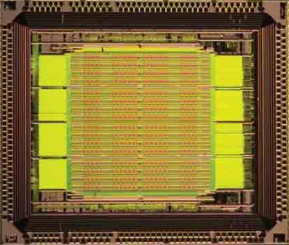
QUICKLOGIC's ViaLink antifuse structure is composed of four metal layers and a tungsten channel covering silicon in the middle. The silicon-covered tungsten channel has the characteristics of high resistance and high capacitance, and acts as an insulating layer between the metal layers, and its resistance is greater than 1 gigaohm. But when the programming voltage is applied to the selected tungsten channel covering the silicon, the silicon will transform into a low-resistance connection with a resistance of less than 50Ω. Because this structure is different from the SRAM type FPGA, it has no configuration memory, so
The programming content is impossible to be read, it is this kind of characteristic that makes this series of chips have a wide range of application prospects in the field of secure communication.
Anti-fuse FPGA can provide better performance for most designs. This is due to the small resistance of its programmable link (anti-fuse contact resistance is about 50Ω), and it has good wiring flexibility and will not hinder the signal. Send and take the most direct
Therefore, the chip speed can be greatly improved. As we all know, with the improvement of the process, the flip-flop speed of the SRAM FPGA has been made very high, but the speed of the chip is still limited. The reason is that the signal is transmitted in the process of the chip.
The time-consuming accounts for about 60% of the entire time delay, which limits the speed of the entire chip.
At present, although the monolithic density of anti-fuse FPGAs is lower than that of SRAM FPGAs, most anti-fuse FPGAs still occupy a leading position in the following aspects: The flexibility of the wiring structure makes software tools easier to implement Automatic layout, routing, and when the design is modified, the output pins of the original configuration can be kept unchanged even if the wiring is re-routed. At the same time, the design modification in the anti-fuse FPGA can usually ensure that there is little change in the delay, because the delay of the additional programmable link required when the wiring is changed does not increase much. In addition, the anti-fuse FPGA also has the advantages of low power consumption, strong radiation resistance, and high and low temperature resistance.
Therefore, the characteristics of anti-fuse FPGA make it have a special application in secure communication products. Making full use of the characteristics of anti-fuse FPGA can increase the encryption and decryption speed of the cryptographic algorithm chip. At the same time, the programming content of the anti-fuse FPGA can not be read out, which protects the main algorithm in the cryptographic module and avoids other physical protections, thereby improving The security of the system.
FTTH Fiber Optic Splice Tray is designed to provide a place to store the fiber cables and splices and prevent them from becoming damaged or being misplaced. It is also called a splice enclosure or splice organizer. This device does not contain any technical functions, and the design is simple. Also, Fiber Optic Tray has a very low price for people to afford. However, the importance of fiber splice tray for protecting fibers is significant. And the skills needed for using a fiber splice tray is not as simple as you think.
Made by industrial high-quality ABS plastic, Fiber Optic Cable Tray is provided to place the fiber splice points and pre-terminated for fiber connectivity. The splice tray expands fiber splice capabilities as well as provides the splicing location for fiber optic cables. It can be put into the fiber distribution frame, fiber splice closure, optic terminal box, etc. Sijee offers different shapes of fiber splice tray with or without termination function. Fiber Optic Tray, Fusion Splice Box, Fiber Optic Cable Tray, Splice Tray Optic Fiber are available.
Applications:
Fiber splice trays are usually placed in the middle of a route where cables are required to be joined or at the termination and patch panel points at the end of the cable runs. Also, splices can be placed in a splice tray which is then placed inside a splice closure for OSP (outside plant) installations or a patch panel box for premises applications. As for indoor application, fiber splice trays are often integrated into patch panels to provide for connections to the fibers.


Fiber Optic Tray,Fusion Splice Box,Fiber Optic Cable Tray,Splice Tray Optic Fiber
Sijee Optical Communication Technology Co.,Ltd , https://www.sijee-optical.com