For the decline in net profit, Ganzhao Optoelectronics said that the price of the chip has a large decline compared with the price of the same period last year, and the chip gross margin has been reduced. For the future development, Ganzhao Optoelectronics said that the company will continue to do two major categories of "LED epitaxial wafers and chips and GaAs solar cell epitaxial wafers and chips".
In terms of business operations, on the one hand, it makes full use of raised capital investment projects, and promotes the construction of Xiamen fundraising projects in an orderly manner, laying a good foundation for stabilizing and expanding the company's market share; on the other hand, fully mobilizing the enthusiasm of personnel and continuously improving product performance. Optimize product structure, update product categories, and enhance product core competitiveness; will also continue to further consolidate the domestic leading position of triple-junction GaAs solar cell epitaxial wafers, and strengthen efforts to develop products based on the quality of the company's products. Application market.

HDI PCB or High density interconnect PCBs are a way of making more room on your printed circuit board to make them more efficient and allow for faster transmission. It's relatively easy for most enterprising companies that are using printed circuit boards to see how this can benefit them.
High density interconnect (HDI) PCBs represent one of the fastest-growing segments of the printed circuit board market. Because of its higher circuitry density, the HDI PCB design can incorporate finer lines and spaces, smaller vias and capture pads, and higher connection pad densities. A high-density PCB features blind and buried vias and often contains microvias that are .006 in diameter or even less.
The copper is the circuits material and the circuits designed by the PCB designers. Depends on the current in the circuits, the PCB copper thickness could be done with 0.5oz-10oz. But the PCB designers need be noted that the copper track width/space need be enlarged with the thickness. For example, the minimum copper track width/space could be 3mil/3mil with 0.5oz, but would be 4mil/4mil with 1oz.
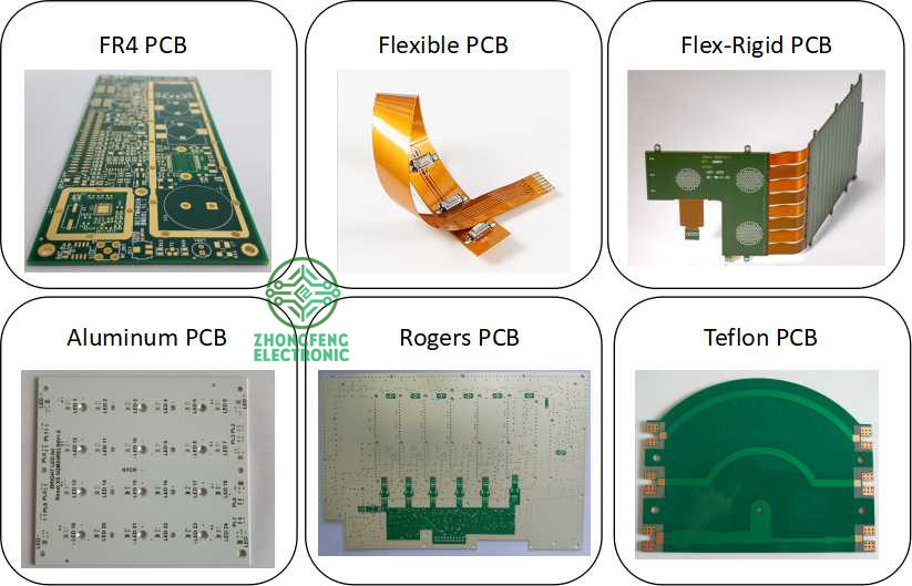
The PCB board could be rigid PCB, could be flex PCB and also could be Flex-Rigid PCB. And the materials could be FR4, PI, Aluminum, Copper-based, Rogers, Teflon, etc. They have different applications. For example, FR4 PCB is the most commonly used for rigid PCB and almost good for all electronics products; PI is the most commonly used for flex PCB; Aluminum and copper-based have good thermal diffusivity and always used for LED PCB ; Rogers PCB and Teflon PCB are always used for High Frequency PCB, etc.
PCB Manufacture Capabilities
|
Features |
Capabilities |
|
Layers |
1-36 layers |
|
Material |
FR-4, Aluminum, Copper, Polyimide, high frequency (Rogers, PTEE, PI), etc. |
|
PCB Type |
FR-4 Standard PCB , Aluminum PCB , Copper-based PCB, HDI PCB, Rigid-Flex PCB, Flex PCB, Thick Copper PCB and Rogers PCB, etc. |
|
Board Thickness |
0.1mm-6.0mm |
|
Copper Thickness |
1/2oz-6oz(18um-210um) |
|
Biggest Board size |
600mm*1200mm |
|
Min Tracing/Spacing |
0.075mm/0.075mm (3mil/3mil) |
|
Min drilling Hole diameter |
0.15mm(6mil), 0.1mm(4mil)-laser drill |
|
Solder Mask |
Green, Black, White, Red, Yellow, Blue and Purple, etc. |
|
Silkscreen color |
White, Blue, Black, Red, Yellow |
|
Surface finish |
HASL Lead free, Immersion Gold (ENIG), Immersion Tin, Immersion Silver, OSP, Carbon oil, etc. |
|
Special Techniques |
Impedance Control, Gold Fingers, Blind/Buried vias, Peelable solder mask, Half holes, Via-in-Pad and Countersink hole, etc. |
PCB Products Show

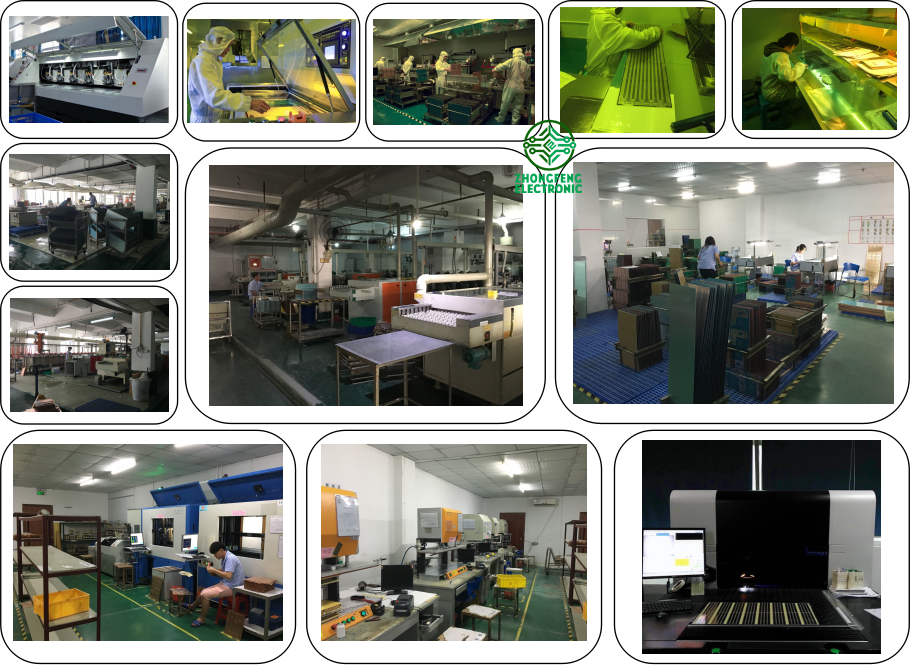
PCB Factory Show

HDI PCB
HDI PCB,HDI Microvia PCB,Prototype HDI PCB,HDI PCB Circuit Board
ZhongFeng Electronic Technology Co., Limited , https://www.dopcba.com