Through our previous article in the SiC series, "SiC material in the end "cool" where? "We learned about the excellent performance of SiC materials. Then, what makes a device made of SiC? Let's take a closer look.
First, where is CoolSiCTM better than Si IGBTs?
At present, IGBTs and MOSFETs are widely used power devices, especially IGBT applications in the high-voltage power electronics are more common. So what's the difference between IGBT and MOSFET? In fact, their structures are very similar. The polysilicon and drift region are used to form the metal-oxide-semiconductor structure as the gate; the N-type doped semiconductor is commonly used in the drift region to withstand the blocking voltage; the gate has a positive pressure (higher than With the device's threshold voltage, the device conducts and the on-state current flows longitudinally in the drift region. The main difference is that the IGBT has a P+ implant as the collector on the back of the drift region, while the MOSFET directly deposits the metal on the back of the N drift region as the drain. The P+ on the back of the IGBT determines that it is a bipolar device. When the device is turned on, the emitter injects electrons, and the collector injects holes. Both carriers participate in conduction. When the device is turned off, excess holes can only be recombined in the body, resulting in tail currents, increased turn-off losses, and limited switching frequency. And at high temperatures, the tail current is more pronounced, resulting in greater turn-off losses. At present, the switching frequency of the IGBT system can be achieved below 100kHz. The MOSFET only relies on electrons to conduct electricity. When the MOSFET is turned off, the electrons can be quickly pumped away. There is no trailing current, and therefore the turn-off loss is smaller and does not substantially change with temperature.
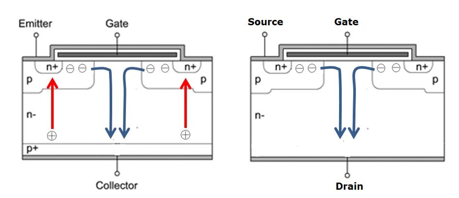
Figure 1 IGBT and MOSFET sectional structure
Below we use the actual test data to intuitively experience the advantages of SiC.
Switching loss
Figure 2 shows the comparison of the switching losses of the 1200V HighSpeed3 IGBT (IGW40N120H3) and the CoolSiCTM MOSFET (IMW120R045M1) on the same platform. Bus voltage 800V, drive resistor RG = 2.2Ω, drive voltage 15V/-5V. Use a 1200V/20A G5 Schottky diode IDH20G120C5 as a freewheeling diode. During the turn-on phase, with a current of 40A, the turn-on loss of the CoolSiCTM MOSFET is about 50% lower than that of the IGBT, and it hardly changes with the junction temperature. This advantage is even more pronounced during the shutdown phase where the turn-off loss of the CoolSiCTM MOSFET is approximately 20% of the IGBT at a junction temperature of 25°C. At a junction temperature of 175°C, the turn-off loss of the CoolSiCTM MOSFET is only 10% of that of the IGBT ( Turn off 40A current). And the switching loss temperature coefficient is very small.
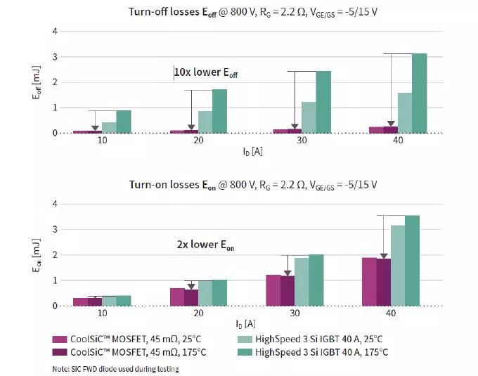
Fig. 2 Switching losses of IGBT and CoolSiCTM
Conduction loss
Figure 3 compares the output characteristics of a 1200V HighSpeed3 IGBT (IGW40N120H3) with a CoolSiCTM MOSFET (IMW120R045M1). At room temperature, the two devices have the same turn-on voltage drop at 40 A. When it is less than 40A, the CoolSiCTM MOSFET exhibits nearly resistive characteristics, while the IGBT has an inflection point in the output characteristics, generally 1V to 2V, and the current linearly increases with voltage after the inflection point. When the load current is 15A, the forward voltage drop of CoolSiCTM is only half that of the IGBT at room temperature. At a junction temperature of 175°C, the forward voltage drop of the CoolSiCTM MOSFET is about 80% of the IGBT. In practical device designs, CoolSiCTM MOSFETs have lower conduction losses than IGBTs.

Figure 3 Comparison of conduction losses of CoolSiCTM and IGBT
Body diode freewheeling characteristics
The intrinsic diode of the CoolSiCTM MOSFET has similar fast recovery characteristics as the SiC Schottky diode. At 25°C, its Qrr and G5 SiC diodes at the same current level are nearly equal. However, both the reverse recovery time and the reverse recovery charge increase as the junction temperature increases. From Figure 4(a) we can see that the Qrr of the CoolSiCTM MOSFET is slightly higher than the G5 Schottky diode when the junction temperature is 175°C. Figure 4(b) compares the intrinsic diode performance of the 650V 41mΩ Si MOSFET intrinsic diode and the CoolSiCTM MOSFET. The 1200VCoolSiCTM MOSFET body diode has only 10% of the Si MOSFET body diode Qrr at normal temperature and high temperature.
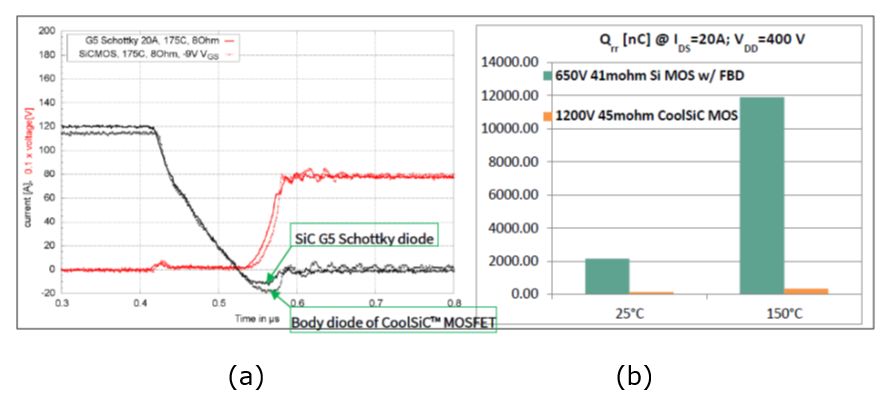
Figure 4 Dynamic characteristics of the body diode of CoolSiCTM MOSFET
Second, where is CoolSiCTM better than other MOSFETs?
We have learned that SiC materials have absolute advantages over Si materials in terms of breakdown field strength, thermal conductivity, and saturation electron velocity, but when it forms MOS (metal-oxide-semiconductor) structures, The charge density of the SiC-SiO2 interface is much larger than that of Si-SiO2. The consequence of this is that the electron mobility of the SiC surface is much lower than the bulk mobility, so that the channel resistance is much larger than the bulk resistance and becomes the main component of the on-state specific resistance. ingredient. However, surface electron mobility differs on different crystal faces. At present, common SiC MOSFETs are planar gate structures, and conductive channels are formed on the Si-plane with many defects and low electron mobility. Infineon's CoolSiCTM MOSFETs feature a Trench trench gate structure. The conductive channel transfers from the horizontal plane to the vertical plane, greatly improving the surface electron mobility, making the device easier to drive and longer.
SiC MOSFETs are subjected to high electric field strength in the blocking state. For Trench devices, the electric field concentrates at the corners of the trenches. This is a weak point in the MOSFET withstand voltage design. Infineon has adopted a new asymmetrical trench structure as shown in the figure below. In this structure, the N+ source and P base regions on the left side of the trench form a normal MOS conductive channel; most of the other side of the trench is surrounded by a heavily doped deep P well, in the blocking state. Next, this P-well can weaken the electric field strength applied to the trench gate oxygen; in the reverse freewheeling state, it can act as a fast-recovery diode and has better performance than a conventional MOSFET body diode.
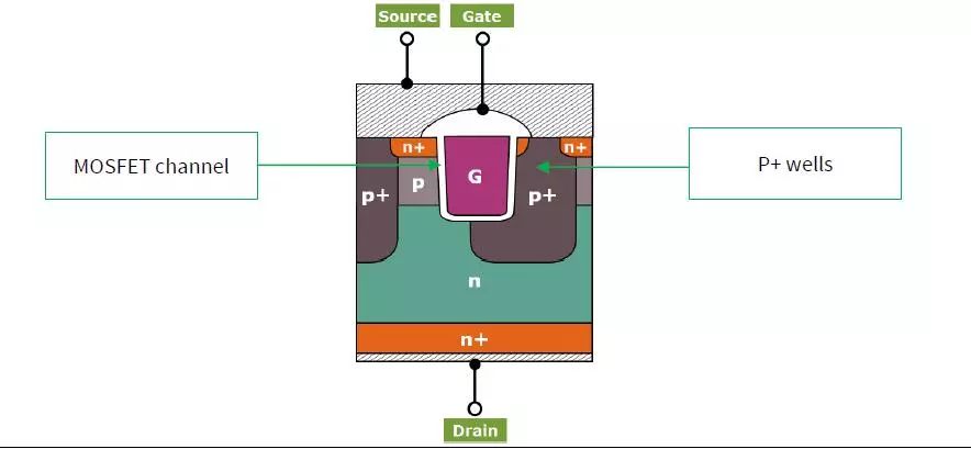
Figure 5 Schematic cross section of CoolSiCTM MOSFET
Compared to other SiC MOSFETs, CoolSiCTM MOSFETs have the following unique advantages
To facilitate replacement of current Si IGBTs, CoolSiCTM MOSFETs are recommended to drive at 15V, which is compatible with current Si-based IGBT driver requirements. The CoolSiCTM MOSFET has a typical threshold voltage of 4.5V, which is higher than the typical 2~3V threshold voltage on the market. A relatively high threshold voltage prevents false triggering due to gate voltage fluctuations.
CoolSiCTM MOSFETs have an optimized ratio of Miller capacitance Cgd to gate-to-source capacitance Cgs, both at the same time as suppressing Miller's parasitic conduction while taking into account the high switching frequency.
Large area deep P wells can be used as fast recovery diodes with very low Qrr and good robustness
CoolSiCTM MOSFETs provide chips, single tubes, and modules for a wide range of products. With a single tube with TO-247 3pin and TO-247 4pin, the Kelvin connection prevents Miller's parasitic conduction and reduces switching losses. Modules include EASY1B, EASY 2B, 62mm, etc., which can cover multiple power level applications. The module uses a low parasitic inductance design, optimized for parallel design, making PCB layout easier
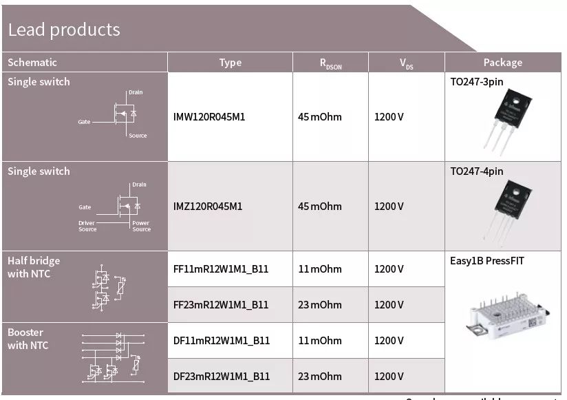
The following is the CoolSiCTM pre-production product catalog
To sum up, CoolSiCTM MOSFET is a reliable technological revolution. With its unique structure and careful design, it will bring users first-class system efficiency, higher power density, and lower system cost. Infineon has always been at the forefront of SiC technology, working hand-in-hand with customers, facing the challenges of the silicon carbide application market, and responding calmly without fear of the future.
Jasminer Machine:Jasminer X4,Jasminer X4-Q,Jasminer X4-1U,Jasminer X4-C 1U,Jasminer X4 BRICK
As a leading brand in the high-throughput server industry, JASMINER has always placed scientific and technological research and product innovation in the highest strategic position and has no upper limit on R&D investment. It is the dedication to technology research and development that enables JASMINER to take the lead in the field of energy saving technology.
At present, JASMINER is one of the world's few cutting-edge computing server brands that apply the core chip technology of "integrated storage and computing". With the chip stacking technology, JASMINER X4, the industry's leading high-throughput computing chip of integrated storage and computing, has overcome Moore's law and led the world. Thus, the energy saving, stability and reliability of the computing power server are further improved.
Based on energy saving, consumption reduction and comprehensive cost optimization, JASMINER X4 series server products have gained strong competitiveness in green environment protection, cost reduction and efficiency improvement for global customers. X4 products based on high-throughput chip architecture, with strong computing performance and excellent energy efficiency, fully meet the needs of green computing, for the development of the new generation of information technology to provide a powerful new data infrastructure guarantee.
Jasminer Machine,X4 1U Etc Miner,jasminer miner,X4 1U 520Mh Miner,jasminer x4
Shenzhen YLHM Technology Co., Ltd. , https://www.hkcryptominer.com