The following analysis is based on the xilinx 7 series
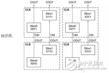
CLB is the basic logical unit of xilinx. Each CLB contains two slices. Each slice consists of 4 (A, B, C, D) 6 input LUTs and 8 registers.
Two slices in the same CLB have no direct line connections and belong to two different columns. Each column has an independent fast carry chain resource.
Slices are divided into two types SLICEL, SLICEM. SLICEL can be used to generate logic, arithmetic, and ROM. In addition to the above functions, SLICEM can also be configured as a distributed RAM or a 32-bit shift register. Each CLB can contain two SLICELs or one SLICEL and one SLICEM.
The 7 series LUT contains 6 inputs A1 - A6 and two outputs O5 , O6 .
It can be configured as a 6-input lookup table, and O6 is now an output. Or two 5-input lookup tables, A1-A5 as input A6 pull high, O5, O6 as output.
A LUT consists of 6 inputs with a logical capacity of 2^6 bits. It requires 2^7 capacity for 7-input logic, and the same for more inputs. Each SLICES has 4 LUTs, and 256-bit capacity enables logic for up to 8 bits of input. To achieve this, each SLICES also includes 3 MUXs (Multi-Channel Selector)
F7AMUX is used to generate 7-input logic function for connecting A and B LUTs.
F7BMUX is used to generate 7-input logic function for connecting two LUTs of C and D.
F8MUX is used to generate 8 input logic functions for connecting 4 LUTs
The need to use multiple SLICES for logic greater than 8 inputs increases the latency of the logic implementation.
The four registers in a SLICES can be connected to the output of the LUT or MUX, or bypassed directly without any logic resources. The set/reset terminal of the register is active high. Only the CLK terminal can be set to two polarities, and other inputs need to be inserted into the logic resources to change the level. For example, a low-level reset requires additional logic resources to invert the rst input. However, setting the rising/falling edge trigger register does not incur additional overhead.
Distributed RAMSLICEM can be configured as distributed RAM, and one SLICEM can be configured as RAM of the following capacity
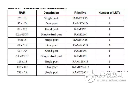
In the case of multiple bits, it is necessary to increase the corresponding multiple LUTs for parallel connection.
The choice of distributed RAM and BLOCK RAM follows the following methods:
1. Less than or equal to 64-bit capacity is implemented in distributed
2. Depth between 64 and 128, if there is no extra block available for distributed RAM. Distributed RAM is required for asynchronous reads. Use block ram when the data width is greater than 16.
3. Distributed RAM has better timing performance than block ram. The distributed RAM is in the logical resource CLB. The BLOCK RAM is in a special memory column, which will cause a large wiring delay and the layout is also limited.
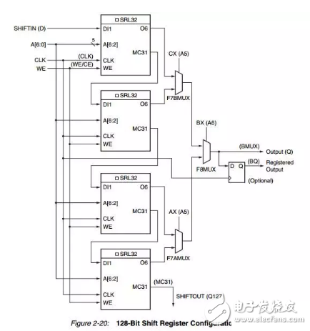
Shift register (SLICEM)The LUT in SLICEM can be set to a 32-bit shift register without using a flip-flop, and the four LUTs can be cascaded into a 128-bit shift register. And it is possible to cascade between SLICEM to form a larger-scale shift register.
One LUT can be configured to 4:1 MUX.
Two LUTs can be configured for up to 8:1 MUX
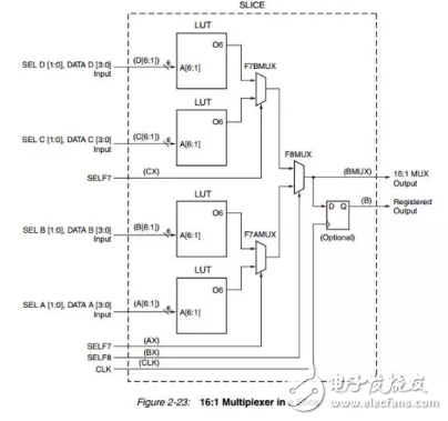
Four LUTs can be configured into 16 MUX
It is also possible to achieve a larger design by connecting multiple SLICES, but since SLICE is not directly connected, wiring resources are required, which increases the delay.
Carry chainEach SLICE has a 4-bit carry chain. Each bit consists of a carry MUX (MUXCY) and an exclusive OR gate that generates carry logic when the adder/subtractor is implemented. The MUXCY and XOR can also be used to generate general logic.
Optical Rotary Sensor,Custom Encoder,Optical Encoder 6Mm Shaft,Handwheel Pulse Generator
Jilin Lander Intelligent Technology Co., Ltd , https://www.jilinlandermotor.com