Application of MC145155 in multi-loop high-resolution frequency synthesizer
Here we introduce a three-loop full-band radio frequency synthesizer composed of a phase-locked loop large-scale integrated frequency synthesizer circuit MC145155. The output frequency of the synthesizer is 76.08 ~ 106.07999MHz, the frequency interval is 10Hz, and the phase jitter is small, and the spectrum purity is high. A single-loop frequency synthesizer that is lower than the phase frequency cannot meet these requirements.
1. Scheme design of three-loop frequency synthesizer
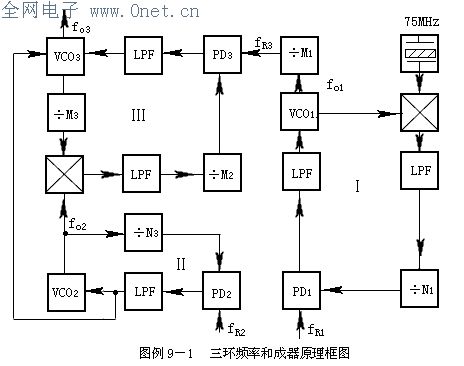
The block diagram of the three-loop frequency synthesis is shown in Figure 9-1. In the figure, ring I and ring II are digital phase-locked loops, and ring III is a frequency addition loop. The output frequency of each loop is
If the frequency step contribution of ring I and ring III to the output frequency fo3 is required to be 10 Hz and 100 kHz, select fR1 = 500 and fR2 = 20kHz, then
If fo3 = 76.08 ~ 106.07999MHz, then calculate
Figure 9-2 shows the principle block diagram of a three-loop frequency synthesizer composed of MC145155.
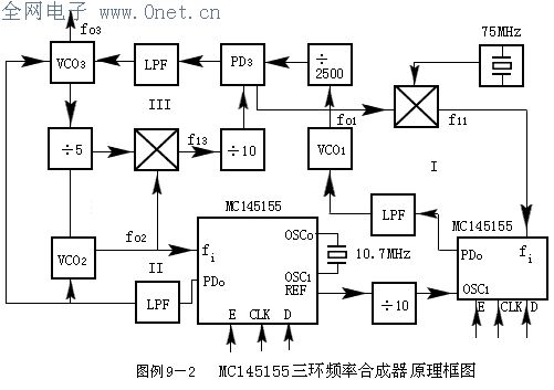
The ring III in the figure inserts a fixed frequency divider N3 = M2 · M3 = 50, and also inserts a mixer. VCO3 uses a JFET push-pull voltage controlled oscillator. In order to ensure accurate and fast locking of ring III, the output control voltage of ring II phase detector is used as the coarse adjustment voltage of VCO3. PD3 uses T4044 (current phase discriminator with ideal integral filter), so loop III is a high-gain second-order loop.
Ring I and Ring II are each composed of a piece of MC145155, and the VCO of the two rings is assumed by an integrated dual voltage control 74S124. Taking ring I as an example, detailed circuit diagram and calculation method are given.
The circuit diagram of ring I is shown in Figure 9-3.
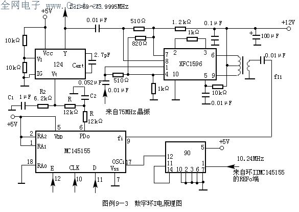
(1) The voltage controlled oscillator VCO1 uses a 74S124STTL circuit. When the control voltage changes from 1 to 4V, the output frequency range is 60 to 85MHz. Therefore, the voltage control sensitivity KV1 is KV1 = 2π × 8.3 × 106rad / s · V
(2) The mixer uses XFC1596 analog multiplier. The balanced input terminals 7, 8 have a bias voltage of 7.2V, and 1, 4 have a bias voltage of 3.97V. The output terminals 6, 9 are coupled by a wide-band transformer (nickel-zinc-ferrite magnetic ring NXO-200φ10 × 6 × 5 winding). The input signal of the mixer is fo1 and the crystal frequency of 75MHz, the output signal frequency is f11 = 6 ~ 1.0005MHz, and it is sent to the fi terminal of MC145155.
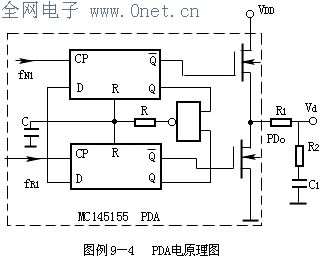
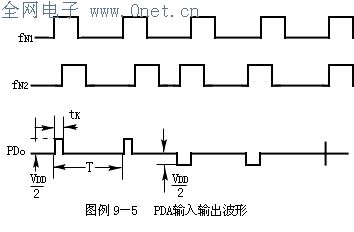
(3) Partial frequency, phase discrimination and loop filter design in MC145155. After fi1 passes the 14-bit programmable frequency divider ÷ N1 in MC145155, it is sent to the phase discriminator PDA in the chip and compared with the reference frequency fR1. The output error signal voltage controls VCO1 to lock the loop. MC145155 internal PDA electrical schematic diagram shown in Figure 9-4. The phase detector waveform is shown in Figure 9-5.
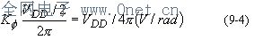
The phase-detection gain Kφ is
The transfer function of the loop filter is
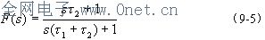
Where τ1 = R1C1, τ2 = R2C1. The loop parameters ωn and ξ are respectively
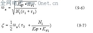
Choose ωn = 2πfR1 / 10, ξ = 1, take N central value N1 = 7000, estimate

Choose C1 = 1μF, then R1 = 24kΩ, R2 = 6.2kΩ.
To improve performance, R1 is divided into two equal-value resistors in series, and the point is connected to C2 to form a T-type low-pass filter. The value of C2 is
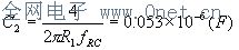
Use 0.047μF and 0.01μF in parallel, as shown in Figure 9-3.
| 3. Way of sending numbers and computer control |
| MC145155 realizes serial sending through three ports of CLK, D and E. Each time 16bit binary code is sent. Among them, the first two digits are function codes, which are directly output as SW1 and SW2, so as to realize band switching or other sending number detection functions. The next 14bit is the ÷ N binary frequency division code to be sent. When the enable terminal E is at a low level, the data of the data line is sent to the shift register under the action of the transition of the clock pulse. When the enable terminal is at a high level, the contents of the shift register are sent to the memory and the 14bit ÷ N copy device to participate in the work of the phase-locked loop. As shown in Figure 9-6. The connection between the MC145155 and the P port of a single-chip microcomputer (MCS-48 series 8748 or MCS-51 series 8551) is shown in Figure 9-7.   As mentioned before, the relationship between the output frequency of the synthesizer and the frequency division ratios N1 and N2 is 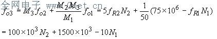 According to the replaceable frequency of this formula, the process is as follows: According to the replaceable frequency of this formula, the process is as follows: The keyboard presses the desired output frequency fo3, and the single-chip program instructions transfer the control words N2, N1 in the memory to the clock in sequence, and then serially send them to the ring II, ring IMC145155 data memory. After sending E = 1 signal, N2, N1 data will enter the latch, make the loop count and lock according to the frequency division ratio of N2, N1, VCO3 will output the required frequency fo3. Every time the control word N2 of the loop II increases by 1, the VCO3 frequency goes into 100kHz, so that the output loop enters the required frequency deviation. Each time the control word N1 of the ring I increases by 1, the frequency of the VCO3 is stepped by 10 Hz, so that the synthesizer achieves a high resolution with a step interval of 10 Hz. |
Power Adpater,Power Adapter Ac To Dc,Ac Dc Adapter,Desktop 5V 3A Power Adapter
ShenZhen Yinghuiyuan Electronics Co.,Ltd , https://www.yhypoweradapter.com